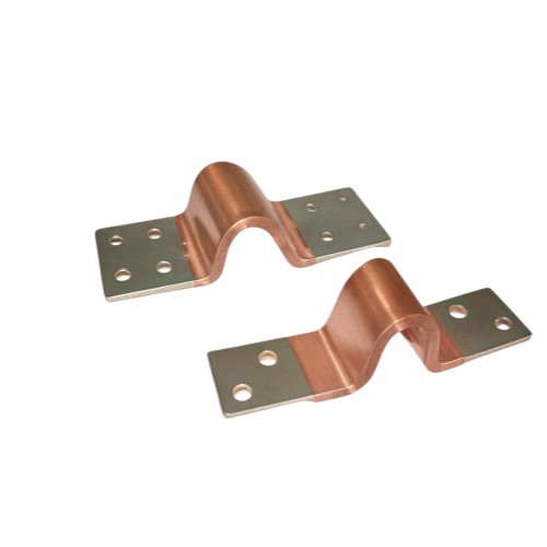
Cu-Al Composite Metal Stamping
Cu-Al Composite Stamping Manufacturing Capability
| Applicable Materials | Copper-Aluminum Clad Metal (Cu-Al Composite), Copper Clad Aluminum (CCA), Cu-Al Transition Joints |
| Sheet Thickness Range | 0.5–6.0 mm (typical); 0.3–10.0 mm (custom) |
| Dimensional Tolerance | ±0.1 mm (typical); ±0.05 mm (precision) |
| Process Types | Single-station die (primary); Compound die; Progressive die (for high volume) |
| Die Steel | SKD11, DC53, Tungsten carbide (YG20 / YC20C) |
| Die Life | ≥200,000 strokes (single-station); ≥500,000 strokes (progressive) |
| Stamping Speed | 30–80 SPM (single-station); 200–600 SPM (progressive) |
| Press Tonnage Range | 25T–400T |
| T1 Lead Time (Single-Station Die) | 2–3 weeks |
| Surface Finish | Ra 0.8–3.2 µm (as stamped); optional: Tin / Nickel / Silver plating on copper side |
| Plating Options | Tin (1–10 µm), Nickel (1–5 µm), Silver (0.5–3.0 µm) – selective plating on copper side only |
| Secondary Operations | Deburring, tumbling, selective plating, annealing (if required), inspection |
| Quality Standards | ISO 9001, IATF 16949 (automotive), RoHS / REACH compliant |
Material Selection & Preparation
Raw Material: Select a Cu-Al composite sheet (explosion-welded, roll-bonded, or friction-welded) with the required copper-to-aluminum thickness ratio. Common ratios are 1:1, 1:2, or 1:5 depending on conductivity and cost requirements.
Material Inspection: Verify bond strength (peel test or ultrasonic test) and thickness uniformity before stamping.
Cutting: The composite sheet is cut into blanks of the required size for single-station stamping.
The Stamping Process (Single-Station Die)
Unlike progressive dies, a single-station die performs all operations in one press stroke, or in a sequence of manually fed operations.
Step 1 – Blanking & Piercing: The outer profile of the connector is cut, and mounting holes are punched in a single stroke. The die must be designed to handle the different shear strengths of copper and aluminum.
Step 2 – Forming / Bending: The blank is placed into a forming die. A punch and die create the arch or bend with the proper radius to avoid cracking at the interface.
Step 3 – Coining / Flattening (Optional): The contact areas may be coined to improve flatness and surface finish for better electrical contact.
Step 4 – Cut-off / Separation: If multiple parts are stamped from one blank, they are separated.
Post-Stamping Operations
Deburring: Remove burrs from punched holes and edges, especially on the copper side, to ensure safe handling and optimal electrical contact.
Surface Treatment: Selective plating (tin, nickel, or silver) may be applied to the copper side to prevent oxidation and improve solderability.
Cleaning: Remove stamping oil and debris.
Inspection: Verify dimensions, bond integrity, and surface quality.
Quality Control (In-Process)
Visual Inspection: Check for cracks, delamination, or separation at the Cu-Al interface.
Dimensional Check: Micrometers and optical comparators verify length, width, hole diameter, and bend angle.
Bond Strength Test: Peel test or ultrasonic inspection to ensure the Cu-Al bond is intact after stamping.
Plating Thickness Test: XRF verifies plating thickness on the copper side.
Delamination at the Cu-Al Interface
Challenge: The copper and aluminum layers may separate or delaminate during stamping, especially during shearing, bending, or coining.
Root Cause: Poor bond strength; excessive shear stress; improper die clearance; sharp corners; insufficient material ductility.
Countermeasure: Use high-quality Cu-Al composite material with verified bond strength; optimize die clearance for bimetal shearing; increase bend radii; avoid sharp corners; preheat material if necessary; use a slower stamping speed to reduce impact stress.
Cracking at the Bend / Arch
Challenge: The arch or bend area may develop cracks, especially on the aluminum side, which has lower ductility than copper.
Root Cause: Aluminum is softer and more prone to cracking; bend radius too small; insufficient material thickness; excessive strain.
Countermeasure: Design generous bend radii (typically ≥ 1.5x material thickness); use progressive forming (multiple small bends instead of one large bend); anneal the aluminum side if possible; optimize punch and die radius.
Burr Control & Hole Quality
Challenge: Burrs on punched holes and edges can affect electrical contact, cause short circuits, or injure operators.
Root Cause: Dull cutting edges; improper clearance for bi-metal materials; tool wear.
Countermeasure: Maintain sharp cutting edges; use carbide inserts for high-volume production; optimize clearance for copper-aluminum combination; implement in-process burr inspection; add deburring or tumbling as a secondary operation.
Dimensional Accuracy & Flatness
Challenge: The part may warp or lose flatness after stamping due to the different thermal expansion coefficients and elastic moduli of copper and aluminum.
Root Cause: Residual stress from bonding; uneven material flow during stamping; springback differences between the two metals.
Countermeasure: Use stress-relief annealing before stamping; optimize die design with proper clamping and support; use coining to improve flatness; implement in-process flatness inspection.
Die Wear & Maintenance (Single-Station Die)
Challenge: Stamping Cu-Al composite materials causes faster die wear than stamping single metals due to the abrasive nature of aluminum and the hardness difference between layers.
Root Cause: Abrasive aluminum oxide; high shear stress; insufficient lubrication; improper die material.
Countermeasure: Use tungsten carbide (YG20/YC20C) or high-vanadium tool steel (DC53) for high-wear stations; apply proper lubrication; implement a preventive maintenance schedule; monitor die wear with in-process sensors.
Material Springback & Deformation
Challenge: Copper and aluminum have different springback behaviors, causing dimensional deviation after bending.
Root Cause: Different elastic moduli; residual stress; improper bend radius; insufficient over-bending.
Countermeasure: Use springback compensation in die design; increase bend radius; apply stress-relief annealing; use over-bending techniques; optimize punch and die clearance.
Selective Plating & Masking
Challenge: Plating must be applied only to the copper side, while the aluminum side must be protected from plating solution.
Root Cause: Aluminum is reactive and can be attacked by plating chemicals; masking is difficult on complex shapes.
Countermeasure: Use selective plating with masking fixtures; apply a protective coating to the aluminum side before plating; use brush plating or spot plating for critical areas; verify plating adhesion and coverage.
Industries We Serve
Delivering precision Cu-Al composite material stampings and components across diverse sectors.
New Energy Vehicles (EVs) – Battery pack busbars, cell connectors, and high-voltage distribution modules.
Power Distribution & Switchgear – Cu-Al transition joints, electrical busbars, and transformer terminals.
Battery Packs & Energy Storage – Energy storage rack connectors and battery interconnects.
High-Voltage Electrical Connectors – Bi-metal lug terminals and Cu-Al composite connectors.
Renewable Energy Systems – Solar and wind power busbars and conductive connections.
Industrial Busbars & Conductors – Cu-Al composite busbars and high-current conductive parts.
Other Electrical Transition Joints – Custom Cu-Al composite stampings for specialized applications.
Our Process Flow
DFM Design → Die Manufacturing (CNC / Wire EDM / EDM) → Die Assembly → Trial Run (T1) → Small-Batch Validation → Mass Production
DFM – Review drawings, blank layout, stations, clearance, springback, and Cu-Al interface stress analysis.
Die Manufacturing – CNC, wire EDM, sinker EDM, grinding, heat treatment, coating, inspection.
Die Assembly – Assemble plates, punches, pilots, springs; set clearance for bi-metal shearing and feed.
Trial Run (T1) – Mount die, run samples, check dimensions, burr, angle, delamination; adjust.
Small Batch – 500–5,000 pcs; CPK/PPK, tool wear, bond integrity, plating, PPAP approval.
Mass Production – Stable stamping, SPC, maintenance, selective plating, packaging.
Why Choose Yixing Technology?
Our company excels in meeting these requirements through our advanced process capabilities and expertise:
Ultra-Precision – Critical features (hole diameter, hole pitch, bend angle) must be held within tolerances of less than 0.1 mm for reliable electrical connection. Our machining equipment achieves tolerances of ±2 µm, significantly exceeding stamping-die standards.
Delamination-Free Stamping – The Cu-Al interface must remain bonded without delamination during shearing, bending, and coining. Our molds feature optimized clearances and radii specifically designed for bi-metal materials, enabling clean, delamination-free stamping.
Multi-Process Integration – Blanking, piercing, bending, coining, and cut-off integrated into a single die by our specialist mold designers, turning complex operations into one efficient stamping solution.
High-Tonnage Durability – Cu-Al composites are thicker and require higher tonnage than thin terminals. We build molds from high-rigidity, high-toughness materials such as SKD11, DC53, and tungsten carbide alloys, ensuring durability and long service life.
Bi-Metal Expertise – Different shear strengths, springback behavior, and thermal expansion rates make bi-metal stamping uniquely challenging. Our engineers have extensive experience designing dies specifically for bi-metal materials, ensuring consistent quality and minimal waste.
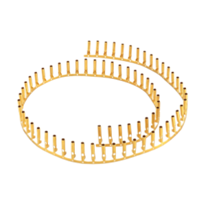
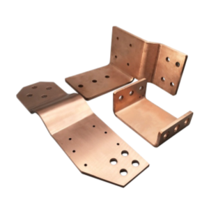
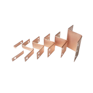
Start Your Quote Here
CATEGORIES
LATEST NEWS
CONTACT US
- Mobile: +8615000908770
- Tel: +86-21-51662821
- WhatsApp: 8615000908770
- Email: contact@yxplasticmolding.com
- Address: Room 323, Building B, Hongchun Business Park, No. 980 Qinghewan Road, Qingpu District, Shanghai