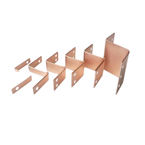
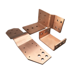
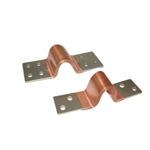
Custom T2 Copper Busbar Components
T2 Copper Busbar Manufacturing Capability
| Applicable Materials | T2 Copper (C11000), T1 Copper, C26000 Brass, C5191 Phosphor Bronze |
| Sheet Thickness Range | 1.0–10.0 mm (typical); 0.5–15.0 mm (custom) |
| Dimensional Tolerance | ±0.1 mm (typical); ±0.05 mm (precision) |
| Process Types | Single-station die; Compound die; Progressive die (for high volume) |
| Die Steel | SKD11, DC53, Tungsten carbide (YG20 / YC20C), High-vanadium tool steel |
| Die Life | ≥200,000 strokes (single-station); ≥500,000 strokes (progressive) |
| Stamping Speed | 20–60 SPM (single-station); 100–300 SPM (progressive) |
| Press Tonnage Range | 100T–1000T |
| T1 Lead Time (Single-Station Die) | 2–3 weeks |
| T1 Lead Time (Progressive Die) | 4–8 weeks |
| Surface Finish | Ra 0.8–3.2 µm (as stamped); optional: Tin / Nickel / Silver plating |
| Plating Options | Tin (1–10 µm), Nickel (1–5 µm), Silver (0.5–3.0 µm), Selective plating |
| Secondary Operations | Deburring, tumbling, CNC machining, selective plating, annealing, inspection |
| Quality Standards | ISO 9001, IATF 16949 (automotive), RoHS / REACH compliant |
1. Material Selection & Preparation
Raw Material: Select a high-conductivity T2 copper plate (C11000) based on current-carrying capacity, mechanical strength, and cost requirements.
Material Inspection: Verify thickness uniformity, surface quality, and mechanical properties (hardness, conductivity).
Cutting: The copper plate is cut into blanks of the required size for single-station stamping.
2. The Stamping Process (Single-Station Die)
For thick-plate copper, single-station dies are often used because of the high tonnage required and the complexity of the L-shaped bends.
Step 1 – Blanking & Piercing: The outer profile is cut, and mounting holes are punched. High-tonnage presses are required to shear through thick copper without cracking.
Step 2 – Forming / Bending: The blank is placed into a forming die. A punch and die create L-shapes with the proper radius. For thick copper, bend radii must be generous to avoid cracking.
Step 3 – Coining / Flattening (Optional): The contact areas may be coined to improve flatness and surface finish for better electrical contact.
Step 4 – Cut-off / Separation: If multiple parts are stamped from one blank, they are separated.
3. Post-Stamping Operations
Deburring: Remove burrs from punched holes and edges to ensure safe handling and optimal electrical contact.
Surface Treatment: Selective plating (tin, nickel, or silver) may be applied to prevent oxidation and improve solderability.
CNC Machining (Optional): For tight-tolerance features or complex geometries, CNC machining may be used after stamping.
Cleaning: Remove stamping oil and debris.
Inspection: Verify dimensions, bend angles, and surface quality.
4. Quality Control (In-Process)
Visual Inspection: Check for cracks, deformation, or incomplete cuts.
Dimensional Check: Micrometers, calipers, and optical comparators verify length, width, hole diameter, and bend angle.
Conductivity Test: Verify electrical conductivity if required.
Plating Thickness Test: XRF verifies plating thickness.
Difficulty 1: Material Sticking & Surface Scratches (Adhesive Wear)
Challenge: Copper has excellent ductility, but it tends to stick to mold surfaces during stamping, leading to burrs, surface scratches, and galling. This is especially problematic for thick plates where friction and pressure are higher.
Root Cause: Copper's softness and high ductility cause it to cold-weld to the die surface; insufficient lubrication; rough tool surface; improper die material.
Countermeasure: Use DC53 mold steel and heat-treat it to improve surface finish and reduce sticking. Apply proper lubrication (copper-specific stamping oil). Polish die surfaces to SPI A1–A2 finish. Consider TiCN or DLC coating for high-wear areas.
Process Tip: DC53 + heat treatment + proper lubrication = reduced sticking and improved surface quality.
Difficulty 2: High Blanking Force & Die Strength
Challenge: For thicker sheets (4mm or more), the blanking force is huge, requiring extremely strong molds. Insufficient die strength can lead to die breakage or deformation.
Root Cause: High shear strength of thick copper; insufficient press tonnage; weak die structure; improper die material.
Countermeasure: Use high-strength die materials (SKD11, DC53, tungsten carbide). Increase die plate thickness and use a reinforced die structure. Ensure press tonnage is sufficient (typically 1.5–2x the calculated blanking force).
Process Tip: High-tonnage press + reinforced die structure + high-strength die materials.
Difficulty 3: Work Hardening & Cracking
Challenge: Thick copper work-hardens after cold working, so multiple stamping operations are needed to avoid cracking. Bending or punching also creates stress concentration, which can lead to edge cracks or distortion.
Root Cause: Copper work-hardens rapidly; residual stress from previous operations; insufficient ductility; sharp corners.
Countermeasure: Anneal before stamping (around 400–600°C) to relieve internal stress and restore ductility. Use multiple forming steps with intermediate annealing if necessary. Increase bend radii and avoid sharp corners.
Process Tip: Annealing at 400–600°C before stamping relieves internal stress and prevents cracking.
Difficulty 4: Clearance Control & Springback
Challenge: Clearance control is critical with thick plates. Too little clearance causes the cutting edge to chip easily; too much clearance produces bad burrs. Additionally, springback is significant, affecting bend angles and hole positioning.
Root Cause: High shear stress; material elasticity; improper clearance; die wear; thermal effects.
Countermeasure: Use FEA simulation to analyze stress distribution and design the punch-die clearance (for copper alloys, a gap of about 4%–9% of the material thickness is usually recommended). Design the mold to compensate for springback. Use over-bending techniques.
Process Tip: FEA simulation + optimized clearance (4%–9% of thickness) + springback compensation mold design.
Difficulty 5: Warpage & Dimensional Drift
Challenge: After stamping, thick copper plates tend to warp—especially larger parts—and hole positions and overall dimensions can drift, affecting assembly.
Root Cause: Residual stress from shearing and bending; uneven cooling; material thickness variation; insufficient clamping.
Countermeasure: Perform a leveling process after stamping, or do a second fine stamping to keep accuracy within ±0.02mm. Use stress-relief annealing if necessary. Optimize die design with proper clamping and support.
Process Tip: Leveling + fine stamping + stress-relief annealing = dimensional stability within ±0.02mm.
Difficulty 6: Bending Angle Accuracy (L-Shape)
Challenge: The L-shaped bends in T2 copper busbars must maintain precise 90° angles for proper fit and assembly. Springback and material thickness variation can cause angle deviation.
Root Cause: Material springback; die wear; inconsistent material thickness; insufficient over-bending compensation.
Countermeasure: Use FEA simulation to predict springback and compensate in die design. Apply over-bending (typically 1–3° extra) to offset springback. Use a bottoming or coining process to stabilize the bend angle. Implement in-process angle inspection with optical comparators.
Process Tip: FEA springback prediction + over-bending compensation + in-process angle inspection.
Difficulty 7: Hole Position Accuracy After Bending
Challenge: After L-shaped bending, the relative position of punched holes can shift, affecting assembly with mating components.
Root Cause: Material flow during bending; residual stress; springback; die wear.
Countermeasure: Design the die to punch holes after bending if possible (to avoid hole distortion). Use FEA simulation to predict hole movement. Implement in-process CMM inspection to verify hole position after forming. Optimize the bend sequence to minimize distortion.
Process Tip: Punch-after-bend design + FEA simulation + CMM inspection.
Our Process Flow
DFM Design → Die Manufacturing (CNC / Wire EDM / EDM) → Die Assembly → Trial Run (T1) → Small-Batch Validation → Mass Production
DFM – Review drawings, blank layout, stations, clearance, springback, and thick-plate stress analysis for single-station die design.
Die Manufacturing – CNC, wire EDM, sinker EDM, grinding, heat treatment, coating, inspection.
Die Assembly – Assemble plates, punches, pilots, springs; set clearance for thick plate shearing and single-station feeding.
Trial Run (T1) – Mount single-station die, run samples, check dimensions, burr, angle, cracking; adjust.
Small Batch – 500–5,000 pcs; CPK/PPK, tool wear, flatness, plating, PPAP approval.
Mass Production – Stable single-station stamping, SPC, maintenance, selective plating, packaging.
Why Choose Yixing Technology?
Our company excels in meeting these requirements through our advanced process capabilities and expertise:
Ultra-Precision – To ensure reliable electrical connection and proper fit with mating components, critical features such as hole diameter, hole pitch, and bend angle must be held within tolerances of less than 0.1 mm. This requires single-station dies with superior precision. Our machining equipment achieves tolerances of ±2 µm, significantly exceeding stamping-die standards.
Burr-Free Stamping – To ensure optimal conductivity and flawless plating, T2 copper busbar surfaces must be free of burrs and scratches. Minor burrs can increase contact resistance or cause short circuits. Our single-station dies feature sharp cutting edges and precisely controlled clearances, enabling clean, burr-free stamping.
Crack-Free Bending – Thick T2 copper plates are prone to cracking during bending because of their thickness and low ductility. To ensure optimal conductivity and structural integrity, the bend area must be free of cracks and micro-fractures. Our single-station forming dies feature optimized bend radii and proper clearance, enabling clean, crack-free bending.
Single-Station Die Expertise – For thick T2 copper busbars, single-station dies offer distinct advantages over progressive dies: lower tooling cost, easier maintenance, and greater flexibility for low- to medium-volume production. Our engineers specialize in designing single-station dies that integrate multiple operations—such as blanking, piercing, bending, and coining—into one efficient stamping solution.
High-Tonnage Durability – Because thick T2 copper plates require high tonnage and generate significant impact force, the single-station die must withstand extreme stress. To support continuous, stable operation, we make our dies from high-rigidity, high-toughness materials such as SKD11, DC53, and tungsten carbide alloys, ensuring durability and long service life.
Start Your Quote Here
CATEGORIES
LATEST NEWS
CONTACT US
- Mobile: +8615000908770
- Tel: +86-21-51662821
- WhatsApp: 8615000908770
- Email: contact@yxplasticmolding.com
- Address: Room 323, Building B, Hongchun Business Park, No. 980 Qinghewan Road, Qingpu District, Shanghai