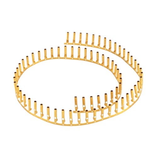
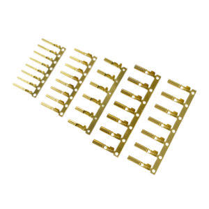
Stamping Reel Copper Terminal / Continuous Copper Strip Stamping
Copper Pin Manufacturing Capability
Applicable Materials: C11000 Copper, C26000 Brass, C5191 Phosphor Bronze, C2680 Brass, C5210 Phosphor Bronze.
Sheet Thickness: 0.2–1.5 mm (typical); 0.1–3.0 mm (custom).
Dimensional Tolerance: ±0.05 mm (typical); ±0.02 mm (precision).
Process Types: Progressive die (primary); compound die; single-station die (+ crimping, forming, coining).
Die Steel: SKD11, DC53, Tungsten carbide (YG20 / YC20C).
Die Life: ≥500,000 strokes (progressive); ≥200,000 strokes (single-station).
Stamping Speed: 200–1,000 SPM (progressive); 30–80 SPM (single-station).
Press Tonnage: 25T–250T.
Lead Time: 2 weeks (single-station T1); 4–6 weeks (progressive T1).
Surface Finish: Ra 0.4–3.2 µm (as stamped); post-plating: Gold / Tin / Nickel.
Plating Options: Gold (0.05–3.0 µm), Tin (1–10 µm), Nickel (1–5 µm), Selective Gold Plating.
Secondary Operations: Deburring, tumbling, selective plating, reeling, coining.
Quality Standards: ISO 9001, IATF 16949 (automotive), RoHS / REACH compliant.
Material Selection & Preparation
Raw Material: Select a master coil of copper alloy (e.g., C2600 Brass or C5191 Phosphor Bronze) based on required conductivity, spring properties, and mating force, typically 0.2–0.5 mm thickness.
Pre-Plating (Optional): The coil may be pre-plated with nickel or tin before stamping to improve corrosion resistance and solderability.
Loading: Load the coil onto a de-reeler and feed it into the progressive die press.
The Stamping Process (Inside the Progressive Die)
The die has multiple stations. With each press stroke, the strip advances one station (pitch), and the machine performs a specific operation.
Station 1 – Piercing (Pilot Holes): Small holes are punched along the carrier strip for accurate feeding and alignment.
Station 2 – Notching & Trimming: The outer profile of the pin is cut, defining the pin width and carrier strip shape.
Station 3 – Pilot & Forming: Pilot pins lock the strip; the pin tip is coined or swaged to smooth edges and achieve the required profile.
Station 4 – Pin Body Forming (U-Shape or Round): The pin body is bent or rolled into a "U" shape or cylindrical form, depending on the connector design.
Station 5 – Pin Closing / Crimping: The "U" is curled further into a closed barrel or pin shape around the future wire or mating contact.
Station 6 – Lance & Cut-off: The pin is separated from the carrier strip, or kept on-strip for reel-form delivery.
Post-Stamping Operations & Quality Control
Cleaning: Stamped strips pass through a chemical bath to remove stamping oil residue.
Plating: Selective gold, tin, or nickel plating is applied to the contact area for conductivity and corrosion resistance.
Reeling: Finished strips are rewound onto reels for shipping and automatic crimping machines.
Visual Inspection: Cameras check for missing material, deformation, or incomplete cuts.
Dimensional Check: Micrometers and optical comparators verify pin length, width, and diameter.
Plating Thickness Test: X-ray fluorescence (XRF) verifies gold/tin/nickel plating thickness.
Manufacturing Difficulties & Countermeasures
1. Pin Deformation & Bending – Thin pins may bend, twist, or deform during stamping, especially at barrel forming and cut-off. Cause: insufficient support, improper clearance, excessive stripping force. Fix: precise stripper guidance, optimized punch-die clearance, reduced stripping force, stress-relief annealing, generous bend radii.
2. Burr Control on Contact Surfaces – Burrs affect conductivity and mating force and may cause short circuits. Cause: dull edges, improper clearance, tool wear. Fix: sharp cutting edges, carbide inserts, in-process burr inspection, deburring/tumbling.
3. Dimensional Accuracy of Pin Diameter & Pitch – Diameter and pitch must be tightly controlled. Cause: mold wear, thermal expansion, inconsistent feeding, springback. Fix: high-precision wire EDM, in-process gauging (GO/NO-GO), consistent die temperature, servo feed.
4. Plating Adhesion & Coverage – Plating may flake or under-cover at edges and inside the barrel. Cause: contamination, poor pre-treatment, inadequate thickness. Fix: proper cleaning, selective plating, controlled bath chemistry, stress relief.
5. Die Wear & Maintenance (Progressive Die) – High speeds (up to 1,000 SPM) cause rapid wear. Cause: abrasive alloys, high cycle rates, insufficient lubrication. Fix: tungsten carbide (YG20/YC20C), proper lubrication, preventive maintenance, wear sensors.
6. Material Springback & Stress Cracking – Phosphor bronze may spring back, causing deviation. Cause: high yield strength, residual stress, improper bend radius. Fix: springback compensation, larger bend radius, stress-relief annealing, over-bending.
7. Reeling & Tangling – Pins may tangle or deform during reeling. Cause: improper tension, insufficient interleaf, deformation during winding. Fix: controlled tension, interleaf paper, pre-shipment reel inspection, custom fixtures.
Our Process Flow
DFM Design → Die Manufacturing (CNC / Wire EDM / EDM) → Die Assembly → Trial Run (T1) → Small-Batch Validation → Mass Production
DFM – Review drawings, strip layout, stations, clearance, springback, and carrier strip design for copper pins.
Die Manufacturing – CNC, wire EDM, sinker EDM, grinding, heat treatment, coating, inspection.
Die Assembly – Assemble plates, punches, pilots, springs; set clearance and feed for high-speed progressive stamping.
Trial Run (T1) – Mount die, run samples, check pin dimensions, burr, angle, plating adhesion; adjust.
Small Batch – 500–5,000 pcs; CPK/PPK, tool wear, plating, PPAP approval.
Mass Production – High-speed stamping (up to 1,000 SPM), SPC, maintenance, selective plating, reel packaging.
Why Choose Yixing Technology?
Ultra-Precision – Critical features (pin diameter, pitch, bend angle) held within <0.05 mm. Our machining equipment achieves tolerances of ±2 µm, exceeding stamping-die standards.
Burr-Free Stamping – Sharp cutting edges and precisely controlled clearances deliver clean, burr-free surfaces for optimal conductivity and flawless plating.
Multi-Process Integration – Blanking, bending, coining, barrel forming, and cut-off integrated into a single progressive die by our specialist mold designers.
High-Speed Durability – Molds rated for 1,000+ strokes per minute, built from high-rigidity, high-toughness SKD11, DC53, and tungsten carbide alloys.
Selective Plating Expertise – Precise gold/tin/nickel plating only on the contact area, with plating control integrated into stamping for consistent thickness and adhesion.
Reel-to-Reel Capability – Finished pins delivered on reels, ready for automatic crimping. In-house reeling and interleaf systems prevent tangling, deformation, and surface damage during shipping and feeding.
Start Your Quote Here
CATEGORIES
LATEST NEWS
CONTACT US
- Mobile: +8615000908770
- Tel: +86-21-51662821
- WhatsApp: 8615000908770
- Email: contact@yxplasticmolding.com
- Address: Room 323, Building B, Hongchun Business Park, No. 980 Qinghewan Road, Qingpu District, Shanghai